The AI Chip Race Has a Memory Bottleneck: HBM4 and the Korean Supply Chain
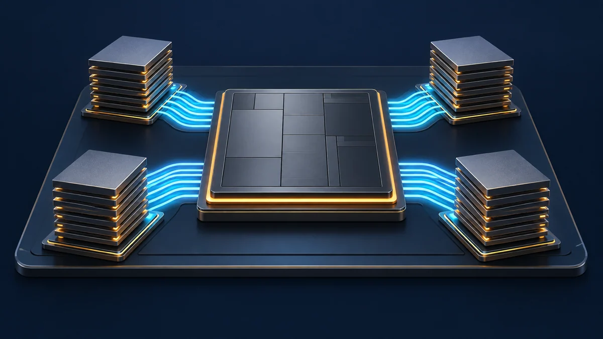
The AI chip race is often reduced to a leaderboard of GPU arithmetic. That misses half of the machine. An accelerator can perform enormous numbers of operations, but its compute units still wait if model weights and intermediate results do not arrive quickly enough. High-bandwidth memory, or HBM, is the stacked memory placed beside the accelerator to keep that data moving.
HBM4 is the 2026 turning point. NVIDIA designed Vera Rubin around it, while Samsung Electronics, SK hynix and Micron are competing on production and next-generation HBM4E samples. Korea is therefore not a peripheral supplier to the U.S. AI buildout. It occupies a critical point connecting accelerator design, foundry production, advanced packaging and the data center.
But saying that HBM is essential is not the same as saying memory alone completes the system. Yield, base-die logic, packaging capacity, heat removal, high-speed interconnects and customer qualification all have to work before a server ships.
Three things to know
- HBM reduces accelerator idle time by feeding large amounts of data through a wide interface close to the compute die.
- HBM4 expands interface width and bandwidth, while making stacking, thermal control and packaging more difficult.
- Vendor speed and efficiency claims must be separated from customer qualification, production yield and measured performance in a complete system.
An AI system is not one kind of chip
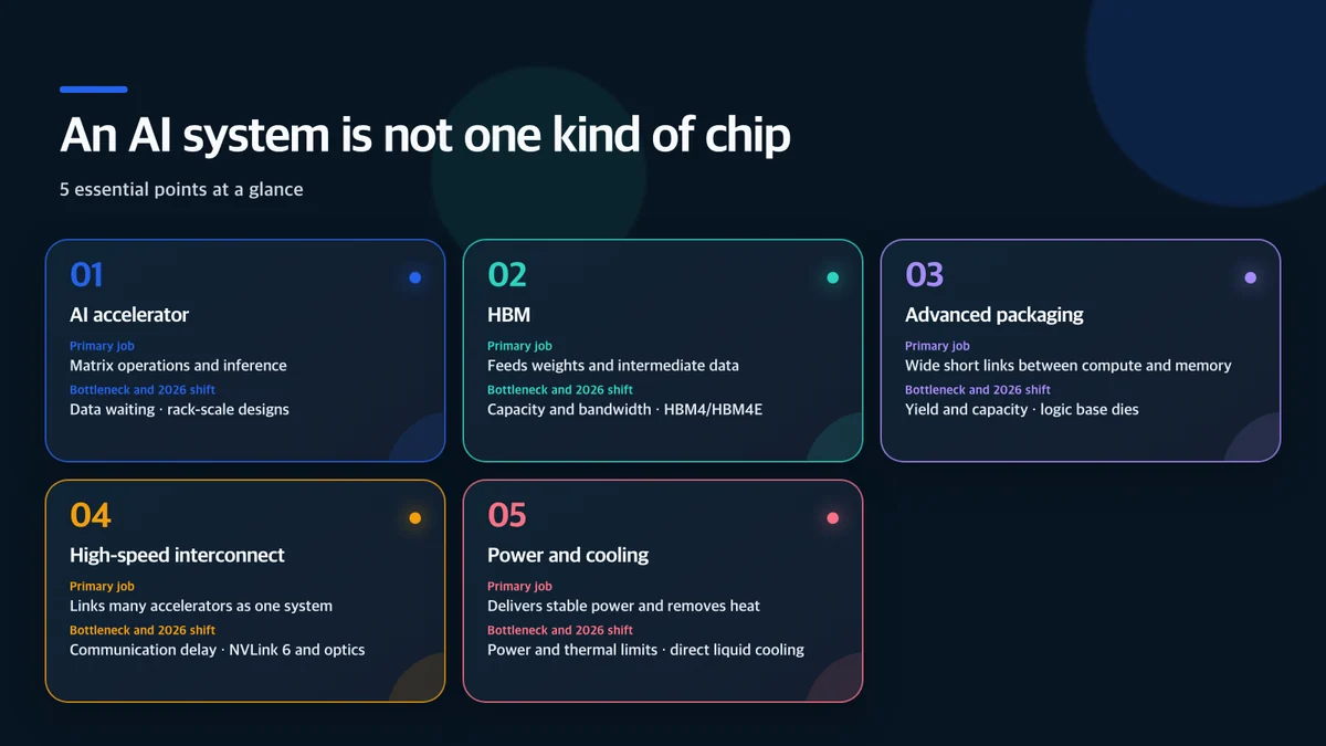
Conventional DRAM usually connects to a processor through modules placed farther away. HBM stacks multiple memory dies vertically and uses through-silicon connections, then places those stacks beside the processor on an advanced package. The design increases not only the speed of each signal but the number of paths operating in parallel.
That performance comes with manufacturing difficulty. The dies have to be thinned, stacked and connected while controlling warpage and heat. An interposer or advanced substrate must link the accelerator to several memory stacks at high yield. Producing enough HBM wafers does not solve the shortage if packaging capacity becomes the next constraint.
A narrow memory path leaves compute waiting
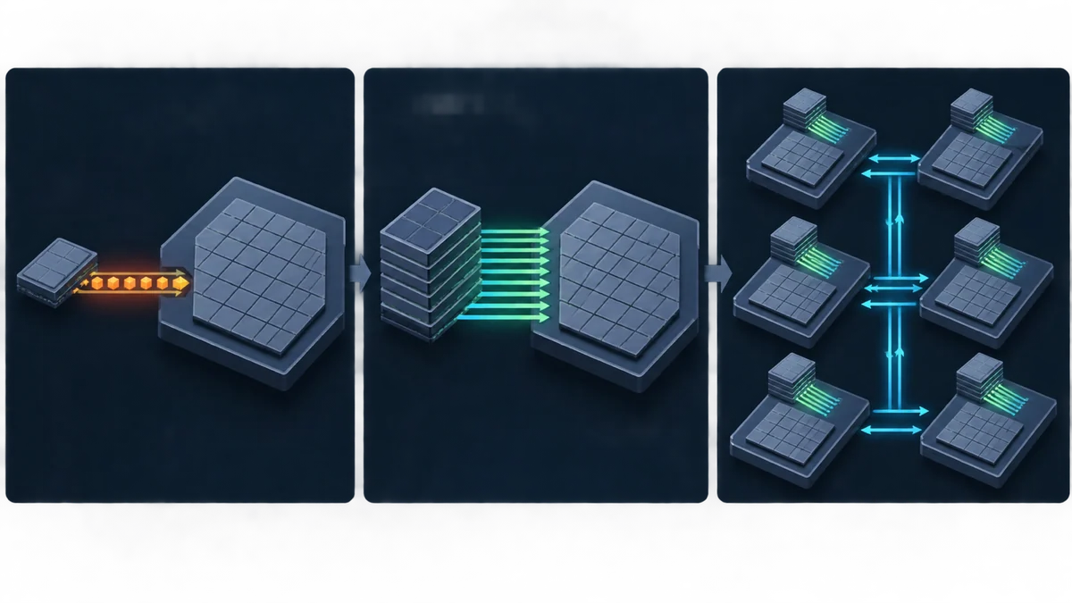
Large-model inference repeatedly reads weights, stores state from earlier tokens and serves many users at the same time. If arithmetic throughput rises faster than memory bandwidth, expensive compute sits idle waiting for data. Long contexts and high concurrency also increase the importance of capacity and efficient movement of the key-value cache.
The NVIDIA Technical Blog description of the Rubin architecture says one Rubin GPU supports up to 288 GB of HBM4 and as much as 22 TB/s of peak memory bandwidth. NVIDIA combines the GPU with NVLink 6, its Vera CPU, networking and a rack-scale design intended for long-running agentic inference and high concurrency.
Those are maximum specifications for a particular platform. They do not mean that one HBM4 stack delivers 22 TB/s, or that an application automatically sustains the theoretical peak. Model architecture, precision, batch size, cache behavior and communication patterns determine how much bandwidth is useful in practice.
Reading Samsung’s HBM4 claims carefully
Samsung said in its February 2026 HBM4 announcement that it had started mass production and commercial shipments. The company reports a sustained data rate of 11.7 Gbps per pin, headroom up to 13 Gbps and up to 3.3 TB/s of bandwidth from one stack.
The 12-layer products range from 24 GB to 36 GB, with a plan to reach as much as 48 GB using 16 layers. Samsung says the product improves power efficiency by 40% and heat dissipation by 30% compared with HBM3E. These are company-reported product figures, not independent measurements of every accelerator or cloud workload.
HBM4 also increases the role of logic in the base die. Samsung combines its 1c DRAM process with a 4-nanometer logic base die. Memory-cell manufacturing, foundry technology and packaging now have to be co-optimized, which helps explain why HBM supply is harder to expand than a simple count of DRAM wafers suggests.
Samsung’s separate partnership announcement with AMD says HBM4 will support AMD Instinct MI455X GPUs and the Helios platform. That link is important for U.S. buyers because it shows memory qualification occurring alongside accelerator roadmaps, not after the GPU has already been designed.
SK hynix is already sampling the next step
SK hynix said in June 2026 that it had shipped 12-layer HBM4E samples to major customers. The company reports up to 16 Gbps per pin, more than 20% higher power efficiency than the previous product and a 17% reduction in thermal resistance.
A sample shipment is not the same milestone as volume production. Customers still test signal integrity, thermals, error behavior, lifetime and compatibility with a specific accelerator. “First sample” matters less commercially than which platforms complete qualification, when sufficient volume becomes available and whether the supplier maintains yield.
It is also difficult to turn Samsung and SK hynix announcements into a simple ranking. Product generation, customer specifications, pin speed, stack height, power conditions and test methods can differ. HBM4E with a customized base die may behave differently across two accelerator designs even when the product family name is similar.
The supply chain from architecture to deployment

A usable accelerator passes through several industries.
- A GPU or ASIC company designs the compute architecture and memory interface.
- Foundries manufacture compute dies and logic base dies for memory.
- Memory companies fabricate DRAM dies and assemble the vertical stacks.
- Advanced packaging joins the accelerator and multiple HBM stacks with short, wide connections.
- Substrates, voltage regulators, networking and cooling turn the package into a server and rack.
- A cloud operator optimizes software and scheduling so the installed hardware produces useful work.
A shortage at any stage can leave finished components waiting elsewhere. HBM shipment forecasts alone therefore cannot measure total AI infrastructure growth, and GPU orders do not reveal the date on which a data center will begin serving customers.
U.S. export controls shape the product as well as the market
Advanced accelerators are industrial products and national-security controls. In January 2026, the U.S. Commerce Department’s Bureau of Industry and Security moved export applications for NVIDIA H200, AMD MI325X and comparable chips to conditional case-by-case review for China. Applicants must address production availability for U.S. customers, buyer compliance and U.S.-based third-party testing.
The Republic of Korea appears on the current Artificial Intelligence Authorization destination list in EAR Part 740. That does not make every transaction automatic. Product classification, end user, installation location, ownership and re-export conditions still matter, and regulations can change between a product announcement and shipment.
Controls can influence design choices, customer screening, data center location and contract language—not only the final destination of a box. Any article, procurement decision or investment analysis should distinguish the rule in effect when a product was announced from the rule in effect when it actually ships.
What Korea contributes and what U.S. buyers depend on
Korea combines two large memory manufacturers with foundry, substrate, packaging, equipment and materials companies. Its 2026 Ministry of Science and ICT plan also calls for securing a cumulative 37,000 GPUs and advancing a domestic K-NPU program. The country is trying to supply global infrastructure while expanding local demand.
For U.S. cloud operators, the connection means that accelerator roadmaps depend on production and qualification far beyond the GPU vendor. For Korean suppliers, it creates exposure to the purchasing cycles of a small group of hyperscalers and accelerator companies. A delayed customer platform, packaging constraint or export-policy change can move revenue even when the memory technology itself works.
Rapid HBM expansion can also affect the wider memory market. Clean-room capacity, advanced process tools and investment capital allocated to premium AI products are not instantly available for ordinary DRAM. That does not guarantee a particular consumer price outcome, but it is one reason AI infrastructure demand can influence the broader semiconductor cycle.
A checklist for evaluating a product announcement
- Is the quoted speed per pin, per stack or for an entire GPU package?
- Does the milestone mean sampling, qualification, mass-production start or revenue shipment?
- What is the baseline and test condition behind an efficiency claim?
- How many layers and how much capacity does the stack provide?
- Which base-die process and packaging method are being used?
- Are packaging, networking, power and cooling constraints included in the claim?
- Are vendor figures clearly separated from independent system benchmarks?
- Have current export controls and end-user restrictions been checked again?
Bottom line
HBM4 is not a supporting detail in the AI race. It determines how quickly an accelerator can receive model data and helps define how much context and concurrency a system can handle. Samsung and SK hynix competing on HBM4 and HBM4E demonstrates how central the Korean supply chain has become to U.S. AI infrastructure.
The winner will not be decided by one headline specification. A supplier has to manufacture at yield, pass qualification on customer accelerators, connect through advanced packaging, control heat and deliver volume on time. The best way to understand the 2026 AI chip race is to treat the GPU, HBM, package, network, power and cooling system as one machine.
Sources and usage notice
- NVIDIA Technical Blog, Rubin GPU architecture — Eduardo Alvarez, Vishal Mehta and Farshad Ghodsian
- Samsung Global Newsroom, commercial HBM4 shipment
- Samsung Global Newsroom, Samsung–AMD memory collaboration
- SK hynix Newsroom, 12-layer HBM4E samples
- U.S. Bureau of Industry and Security, semiconductor export-license review policy
- U.S. Export Administration Regulations Part 740
- South Korean Ministry of Science and ICT, 2026 work plan
This article independently reorganizes product specifications and announcement facts from the sources above. It does not reproduce their photographs, product renders or diagrams. Trademarks and product names are used only to identify the subjects of independent reporting and analysis.