The 2026 AI chip supply chain across Korea the US and Japan
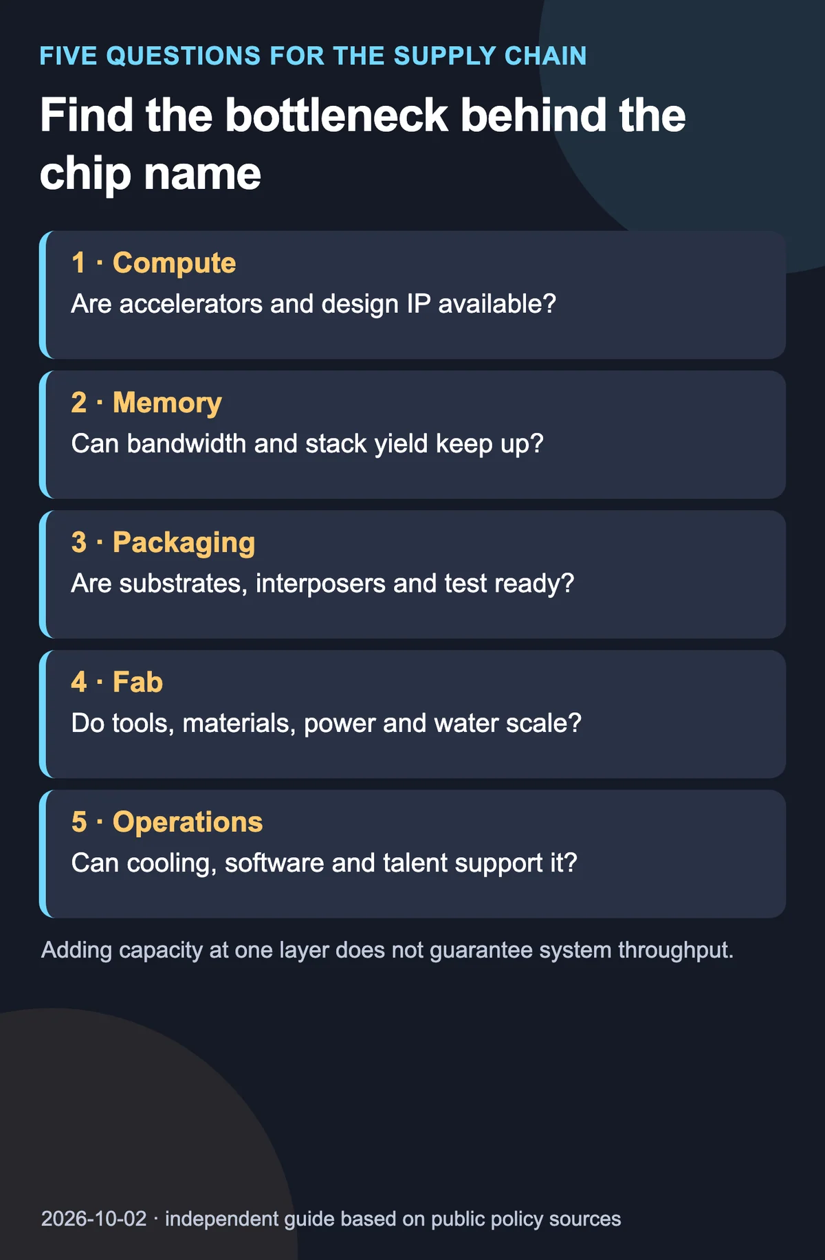
An AI chip supply chain is not a contest to build one famous GPU. An accelerator can sit idle when high-bandwidth memory cannot feed it. Good logic and memory cannot ship without substrates, interposers, bonding, packaging equipment and tests. A finished server still needs power, cooling, networking and software before paid work can use its theoretical compute.
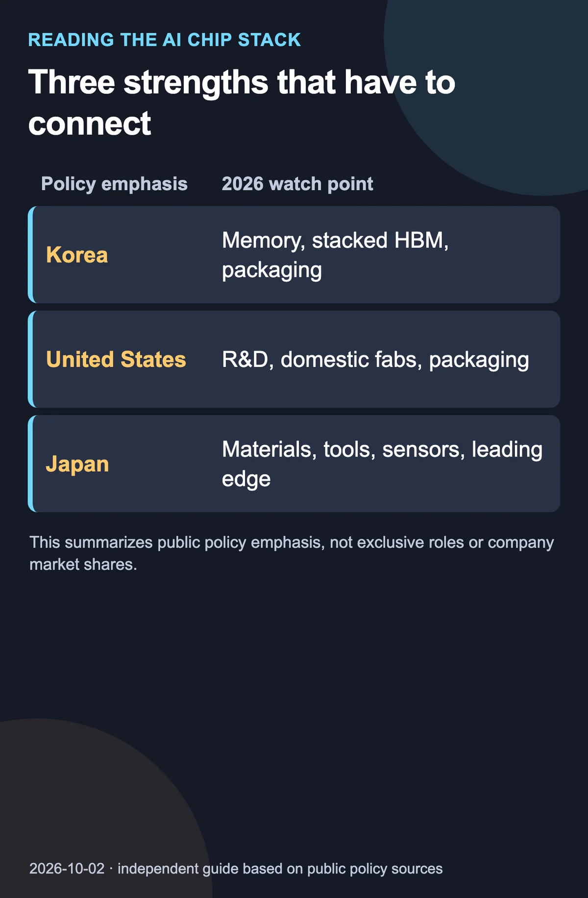
The 2026 strategies of Korea, the United States and Japan reflect different starting points, but not an exclusive division of labor. Korea wants to connect its manufacturing and memory base to design, software and services. The United States is linking domestic fabrication to packaging research and scale-up. Japan is combining long-standing materials and equipment capabilities with an effort to rebuild leading-edge logic production. Companies in all 3 countries participate in multiple layers and manufacture across borders.
This guide therefore compares public-policy emphasis rather than market share or national winners. It also separates a plan, a funding notice, a pilot result and qualified mass production—stages that headlines often compress into one claim.
Unfold an AI system into 7 layers
The stack is easier to reason about when the finished product is taken apart.
- Workload and model: Training, high-volume inference, edge devices and vehicles require different precision, memory capacity and latency.
- Architecture and IP: Accelerator design, CPUs, interfaces, electronic-design tools and verification IP define what can be built.
- Front-end fabrication: Foundries form logic and memory devices on wafers and learn to produce them at usable yield.
- Memory: HBM and other memory have to deliver data rapidly enough to keep compute units occupied.
- Advanced packaging: Chiplets and memory are connected through substrates or interposers while power delivery and heat are managed.
- Materials, equipment and test: Wafers, chemicals, lithography, deposition, etch, bonding, metrology and test support every process step.
- System operations: Servers, networking, electricity, cooling, compilers, frameworks and skilled operators determine real utilization.
Doubling capacity at one layer does not double the completed system. The slowest constraint becomes the bottleneck; removing it often exposes another. That is why factory floor area and investment announcements need to be checked against qualified output, yield, interoperable components and utilization.
Korea sets a goal from chip through service
The Korea Ministry of Science and ICT second-half 2026 work plan, briefed on July 16, describes a “K-AI semiconductor full package ecosystem.” Its stated ambition spans AI chips, infrastructure, networks, software and services developed in Korea, with public-procurement support intended to help early products establish a market.
The breadth matters. A domestic accelerator still needs usable compilers and libraries, server validation, networking and real customer workloads. Conversely, domestic sourcing alone does not prove price, performance, compatibility or reliability. Useful evidence would include repeat purchases, production use, porting time and failures—not only the number of units procured.
The plan also says preliminary planning will be completed in the second half of 2026 before work begins on 1nm-class devices intended to go beyond current physical limits and on stacked next-generation HBM. That language sets a clear boundary: a preliminary-planning target is not a claim that 1nm production or a new HBM generation has been completed. The next things to watch are project scope, budget, participants and the development and validation schedule.
Back-end infrastructure is a separate part of the policy. On February 27, 2026, Korea’s Ministry of Trade, Industry and Resources issued an implementation notice for new advanced-packaging infrastructure projects and invited participating institutions. The notice establishes a program step; it does not report facility utilization or mass-production yield. Follow the equipment installation date, user access, prototypes, reliability work and movement into customer qualification.
The United States treats packaging as essential manufacturing
The US National Institute of Standards and Technology’s National Advanced Packaging Manufacturing Program defines advanced packaging as assembling multiple chips with different functions tightly on a substrate in 2 or 3 dimensions. It can deliver more function, performance and power savings than mounting conventionally packaged chips on a circuit board, but it makes interconnection and validation much harder.
NIST says the first program funding opportunity finalized a combined $300 million for advanced-substrate and materials research by 3 recipients: Absolics, Applied Materials and Arizona State University. That is a disclosed award total and recipient count, not total US packaging investment, revenue or production capacity.
The program frames 4 engineering questions that are useful far beyond the awards.
- Can multiple chips be assembled closely enough to behave like one large traditional chip while retaining production and cost benefits?
- Can the package deliver power and remove heat from tightly coupled devices?
- Can a complex assembly be tested and repaired economically?
- Can reliability be measured when conventional visual inspection cannot see structures at that scale?
Packaging is not a decorative box. Chiplet interconnect, distance to HBM, warpage, bonding yield, thermal behavior and test coverage change system performance and cost. More front-end fabs will not complete an end-to-end domestic supply chain if that layer cannot scale with them.
Japan places ecosystem rebuilding among 17 technology fields
Japan’s Cabinet approved the Integrated Innovation Strategy 2026 on July 14. The annual strategy is intended to put the seventh Science, Technology and Innovation Basic Plan for fiscal 2026 through 2030 into action, with particular emphasis on measures across fiscal 2026 and 2027. Semiconductor and information-communications technologies appear as 1 of 17 important technology fields.
Inclusion in a list of 17 demonstrates policy priority, not production volume or a measured technology lead. Evaluating Japan’s position requires looking at how materials and equipment suppliers, university research, sensors and power devices, leading-edge logic, design talent and overseas customers connect.
A JETRO event report published March 5, 2026 summarizes presentations and interviews around SEMICON Japan 2025. Speakers described Japanese materials, chemicals, equipment and precision manufacturing as strengths. A Yokohama National University speaker also said design and development capabilities remained insufficient and emphasized international collaboration.
Those statements are the views of event participants, not an independently measured national market-share table. Their more useful message is that equipment and materials do not become leading-edge products without joint development, design capability and customers.
The Rapidus company profile lists leading-edge semiconductor research, development, design, manufacturing and sales together with advanced-packaging services. Its timeline says the IIM-1 pilot line started operating in April 2025, electrical characteristics of prototype 2nm GAA transistors were demonstrated that July, and next-generation logic mass production is planned to begin in 2027.
That final date is a company-stated plan. Demonstrating transistor operation is different from producing complete customer designs economically. Yield, a design ecosystem, packaging, reliability, qualification and repeat orders all have to align, so the 2027 entry should not be modeled as guaranteed volume.
National roles overlap even while policy competes
“Korea makes memory, America designs, Japan supplies materials” is memorable and too crude for procurement. Korea also has foundries, fabless companies, equipment and materials. US companies span architecture, equipment, memory and packaging. Japan participates in sensors, memory, design and logic manufacturing as well as tools and materials.
Headquarters, wafer fabrication, packaging, equipment origin and final data-center location can all be in different countries. Map the chain by component instead: accelerator, HBM, interposer, substrate, bonding and test tool, firmware, compiler and cooling system. For each, record the primary source, an alternate, and the qualification time required to switch. An alternate part that needs 6 months of software and reliability work is not immediate redundancy.
Different demand scenarios move the bottleneck
Systems sold under the same AI label can need very different things.
- Frontier training: Large accelerator clusters, HBM, high-speed networking, power and cooling must arrive together. Communication or memory bandwidth can bind before arithmetic does.
- Cloud inference: Hourly demand, response latency, energy cost and scheduling across models matter. Cost per completed request and utilization can matter more than peak specifications.
- Private enterprise inference: Security and integration with existing data dominate. At modest scale, software and operations talent may constrain delivery more than hardware.
- On-device AI: Power, thermals, size, sensor interfaces and unit cost lead. Supply of the highest-end data-center processor does not describe this market.
Demand numbers also need stages. A reservation, a qualification sample, an installed server, an accelerator assigned to production and paid-work utilization are different quantities. Treating cancelable orders as consumed chips or installed capacity as 100% utilized compute can overstate both shortages and final demand.
Six indicators to track after the announcement
Use these measures to connect a policy or factory headline to usable supply.
- Customer qualification and production yield: Look for repeat shipments and the share of wafers or packages meeting saleable performance, not only a working sample.
- Combined HBM and package yield: Memory output is incomplete evidence unless stacking, bonding and thermal steps produce qualified assemblies.
- Substrate, interposer and test lead times: Available wafers cannot become server revenue while back-end slots are missing.
- Tool and material commissioning: Follow delivery, installation, process qualification and utilization—not only equipment orders.
- Power, cooling and network readiness: Compare grid connection and data-center permits with server delivery dates and cooling design.
- Software compatibility and use: Measure whether important models run reliably, how long migration takes and how many hours installed accelerators do useful work.
Export controls, subsidy conditions, currency and energy prices can shift both supply and demand. These rules can change quickly, so check the date, covered item, end-user test and transition period in official documents. A claim that an entire country is simply “blocked” often hides licenses, performance thresholds and use-specific conditions.
The conclusion is a connected chain, not a country ranking
The 2026 sources show 3 policy directions. Korea is building from manufacturing and memory toward a stack that includes software and service, while planning research on next-generation HBM and very small devices. The United States is addressing a missing link through work such as the first $300 million of NIST advanced-packaging awards. Japan places semiconductors and communications among 17 priority fields while trying to connect materials and equipment strength to rebuilt leading-edge logic.
But a plan, program notice, finalized award, prototype, pilot line, customer qualification and mass production are separate stages. Keep them separate and find the slowest layer and switching time. This article is a technology and policy guide, not a recommendation to invest in any company, security or country. Procurement and financial decisions require current contracts, rules, yield and customer evidence beyond the public materials summarized here.